Mentor's Xpedition: Power Up Your PCB Design Process! pcb process flow chart
If you are looking for The Many Ways You Can Easily Ruin Your PCB Antenna Design | Hackaday you've visit to the right page. We have 25 Pics about The Many Ways You Can Easily Ruin Your PCB Antenna Design | Hackaday like The PCB Design Process For Advanced Electronics | Northwest Engineering, PCB Process Flow Chart | www.homillux.com and also IPC 7351 Standards to Design a Footprint | Sierra Circuits. Read more:
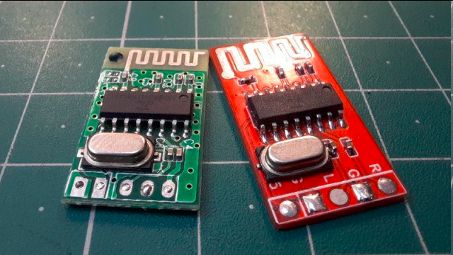
The Many Ways You Can Easily Ruin Your PCB Antenna Design | Hackaday
 hackaday.com
The Many Ways You Can Easily Ruin Your PCB Antenna Design | Hackaday
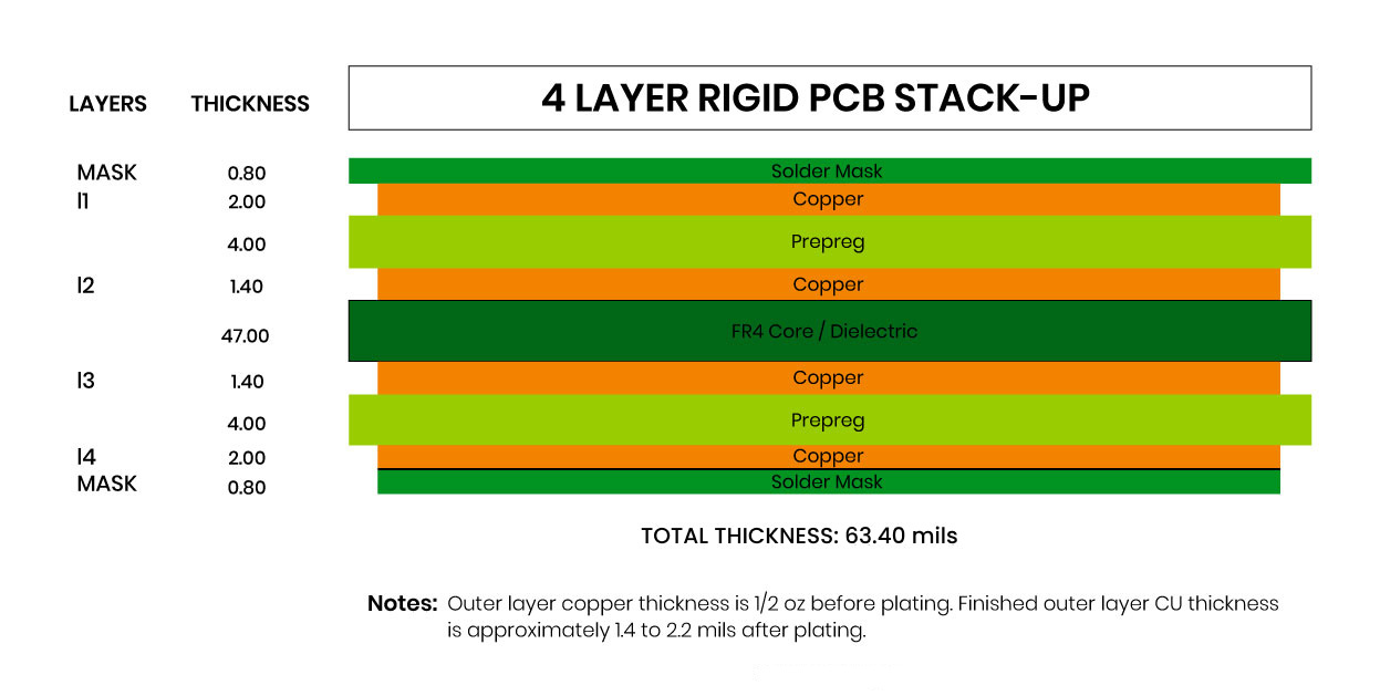
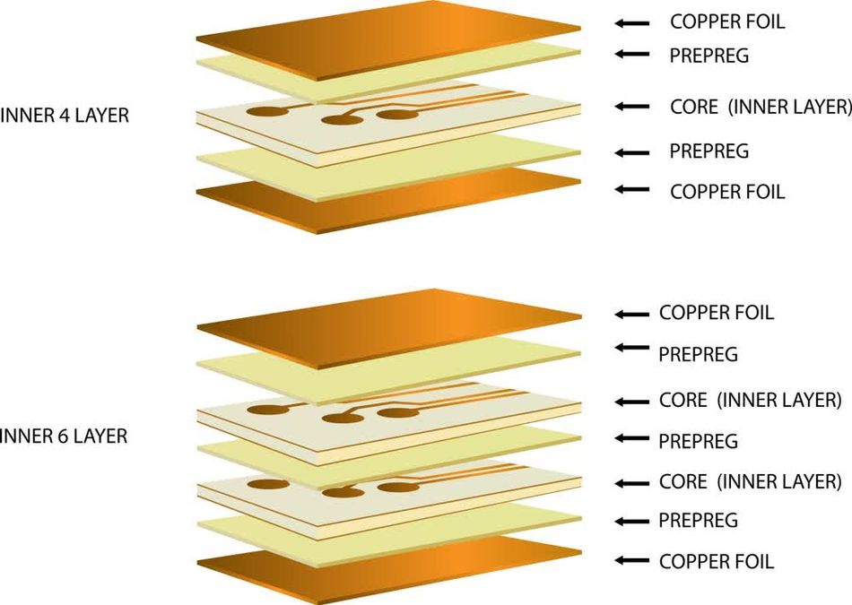
PCB Stack-Up Guide & Examples | San Francisco Circuits
 www.sfcircuits.com
PCB Stack-Up Guide & Examples | San Francisco Circuits
What's New In Xpedition - VX. 2.12 | Siemens Software
 eda.sw.siemens.com
What's new in Xpedition - VX. 2.12 | Siemens Software
Power Supply PCB Designer And Layout Expert
 www.power-supply-designer.com
Power Supply PCB Designer and Layout Expert
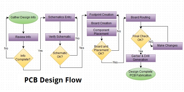
Pcb Design Process Flow At Louise Whipple Blog
 storage.googleapis.com
Pcb Design Process Flow at Louise Whipple blog
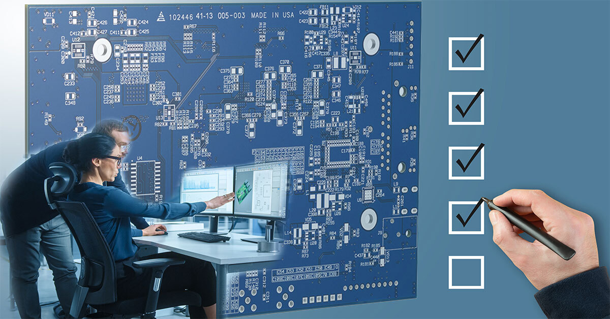
PCB Design Checklist To Build An Efficient Board | Sierra Circuits
 www.protoexpress.com
PCB Design Checklist to Build An Efficient Board | Sierra Circuits
How To Design Your Own PCB – From Basic Layout Tips – PCB HERO
 www.pcb-hero.com
How to Design Your Own PCB – From Basic Layout Tips – PCB HERO
Mentor Graphics Expedition Pcb Free Download - Coolyload
 coolyload166.weebly.com
Mentor Graphics Expedition Pcb Free Download - coolyload
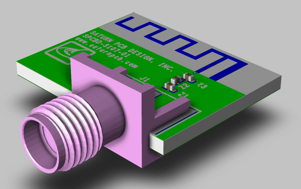
How To Design A PCB Antenna?
 www.nextpcb.com
How to Design a PCB Antenna?
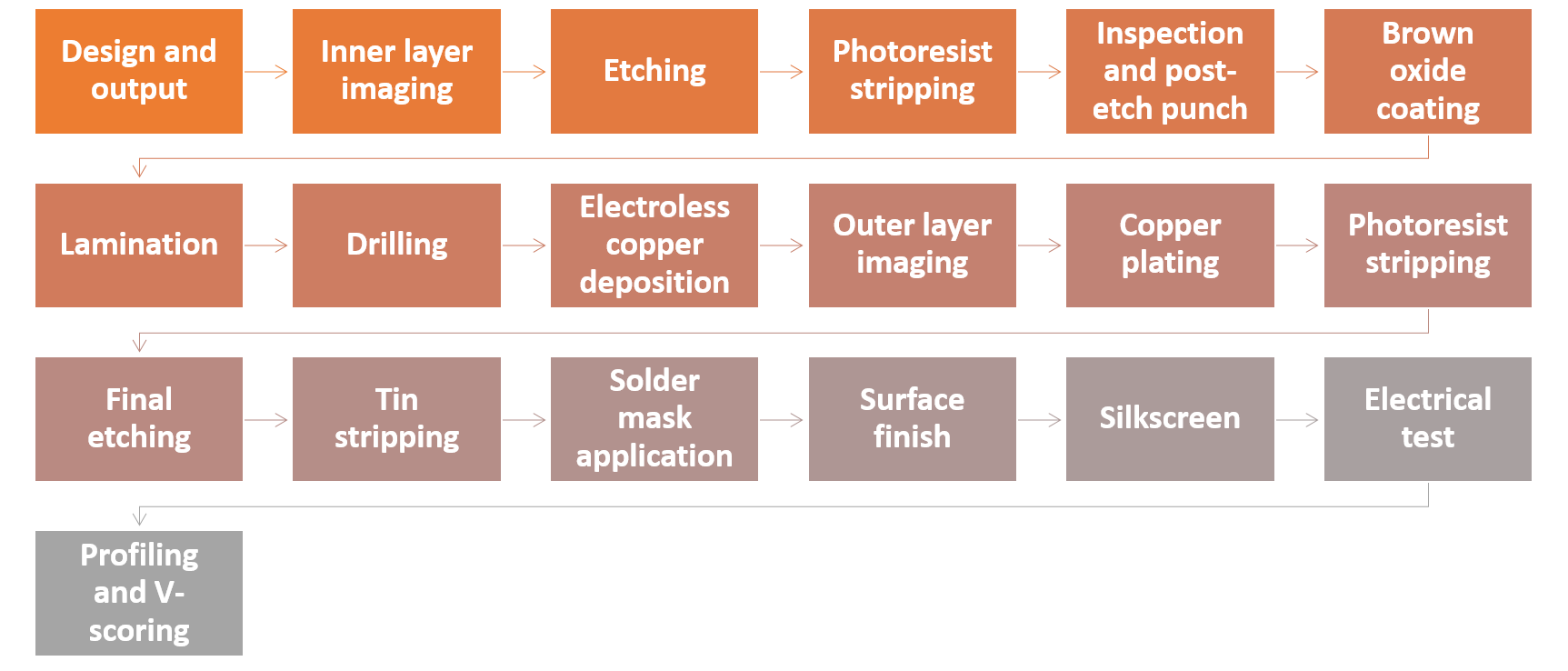
Pcb Process Flow Diagram Let The Experts Talk About : What A
 grisetai8mlibguide.z13.web.core.windows.net
Pcb Process Flow Diagram Let The Experts Talk About : What A
Mentor Graphics Launches New Xpedition Platform To Optimize Advanced
 pcb-copy.com
Mentor Graphics Launches New Xpedition Platform to Optimize Advanced ...
Xpedition PCB Layout Software For Printed Circuit Boards
 pcb-design.pages.dev
Xpedition PCB Layout software for Printed Circuit Boards
PCB Layers: Everything You Need To Know - PCBA Manufacture
 www.dyc-electronic.com
PCB Layers: Everything You Need to Know - PCBA Manufacture
An Overview Of Layer Stack Management In PCB Design, 44% OFF
 www.oceanproperty.co.th
An Overview Of Layer Stack Management In PCB Design, 44% OFF
IPC 7351 Standards To Design A Footprint | Sierra Circuits
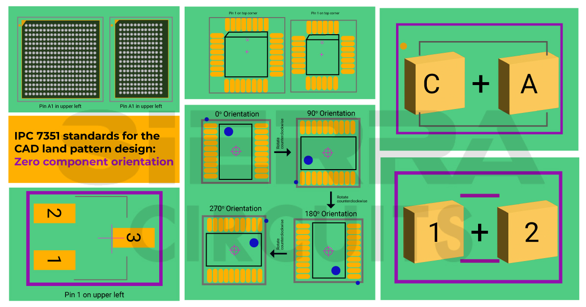 www.protoexpress.com
IPC 7351 Standards to Design a Footprint | Sierra Circuits
Mentor's Valor NPI Fully Integrated With Xpedition PCB Development
 www.eetimes.com
Mentor's Valor NPI Fully Integrated With Xpedition PCB Development ...
Mechanical Keyboard PCB: DIY Custom Keyboard Tutorial-FS PCBA
 www.fs-pcba.com
Mechanical Keyboard PCB: DIY Custom Keyboard Tutorial-FS PCBA
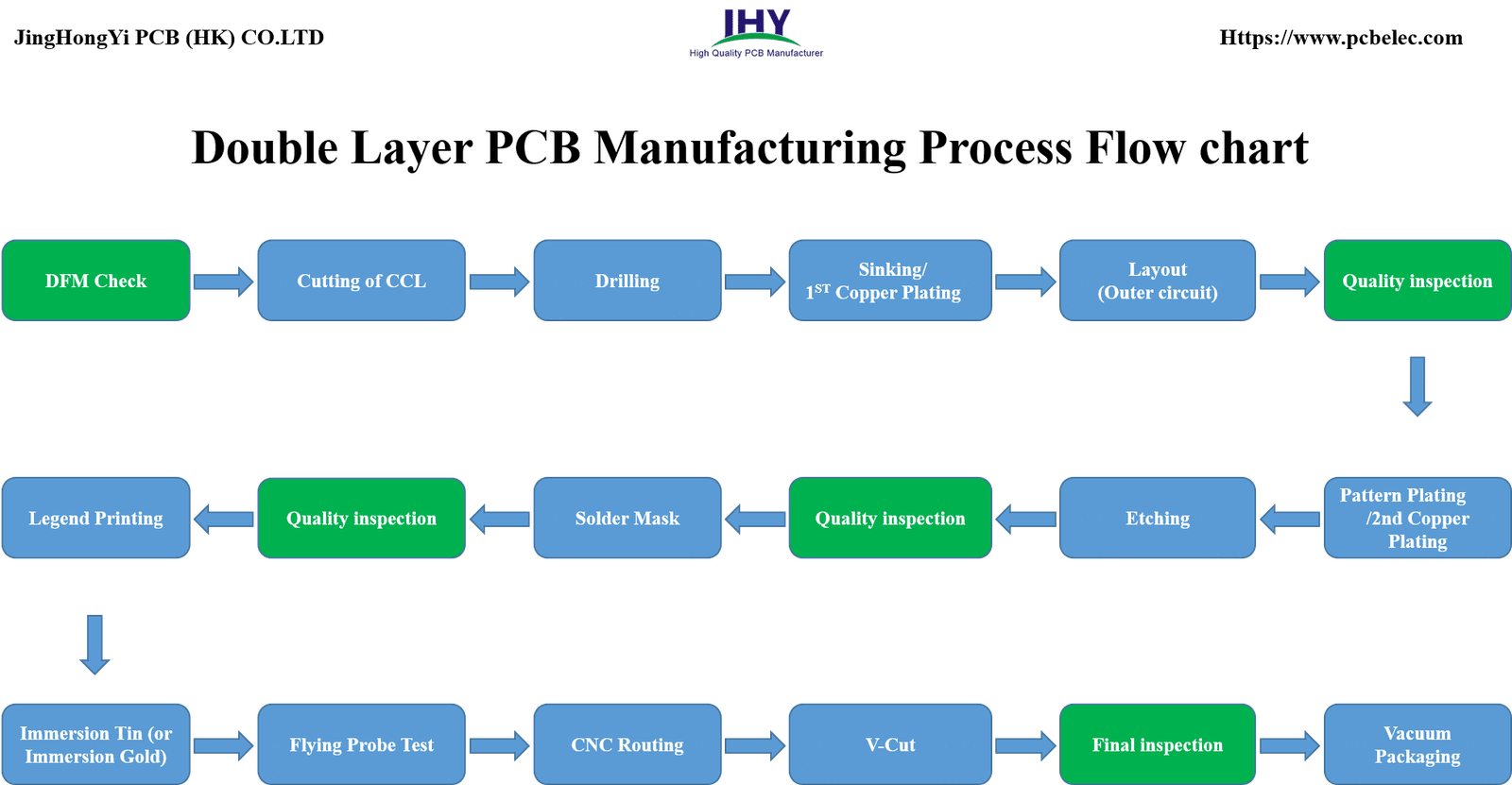
PCB Process Flow Chart | Www.homillux.com
 www.homillux.com
PCB Process Flow Chart | www.homillux.com
6 Layer Pcb Design Guidelines - Design Talk
 design.udlvirtual.edu.pe
6 Layer Pcb Design Guidelines - Design Talk
PCB Process Flow Chart | Www.homillux.com
 www.homillux.com
PCB Process Flow Chart | www.homillux.com
Pcb Design Steps - Design Talk
 design.udlvirtual.edu.pe
Pcb Design Steps - Design Talk
The Importance Of Design For Manufacturability In PCB Design
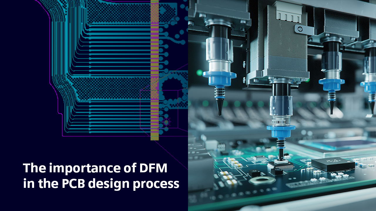 blogs.sw.siemens.com
The importance of Design for Manufacturability in PCB design ...
Siemens Electronic Systems Design & Manufacturing On LinkedIn: Save
 www.linkedin.com
Siemens Electronic Systems Design & Manufacturing on LinkedIn: Save ...
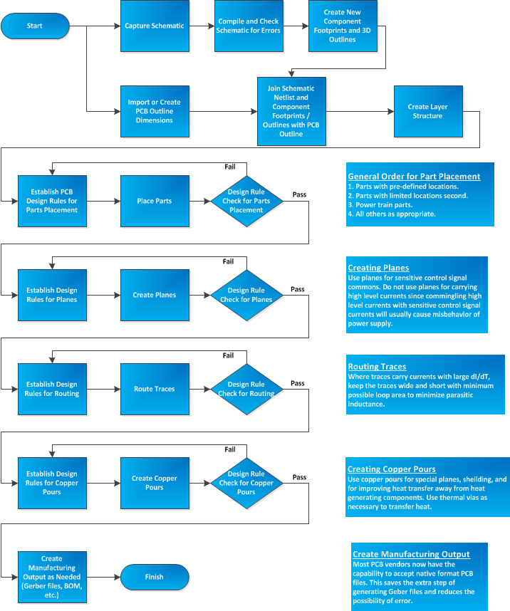
The PCB Design Process For Advanced Electronics | Northwest Engineering
 www.nwengineeringllc.com
The PCB Design Process For Advanced Electronics | Northwest Engineering ...
A Step-by-Step Guide To PCB Manufacturing Process
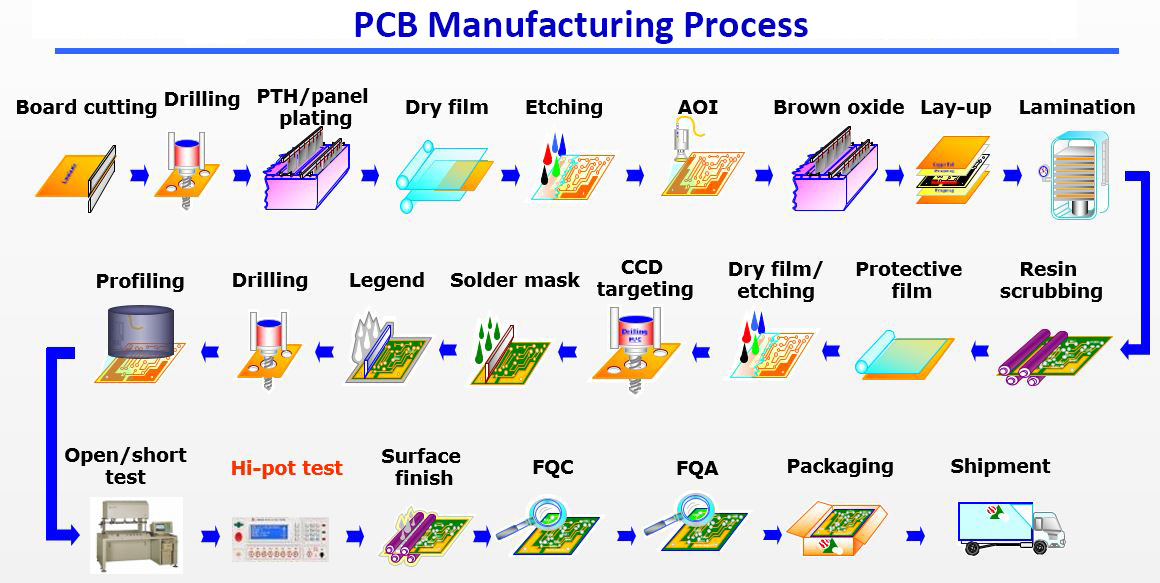 www.nextpcb.com
A Step-by-Step Guide to PCB Manufacturing Process
What's new in xpedition. Ipc 7351 standards to design a footprint. Mentor graphics expedition pcb free download