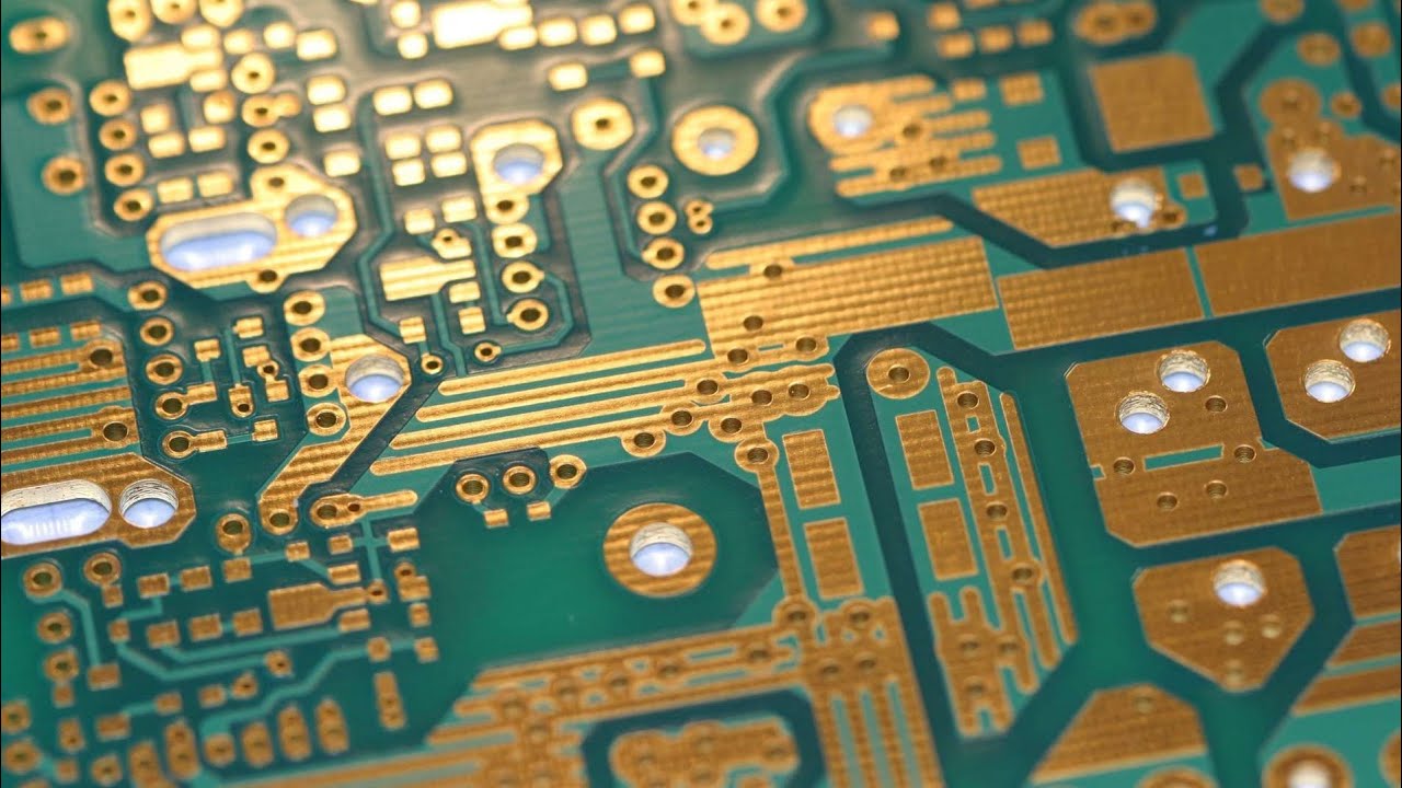
Non-Functional Pads PCB: Via-in-Pad Guidelines for Better PCBs! via in pad guidelines
If you are looking for Top 5 Pcb Design Guidelines In Electronics Industry 2 - vrogue.co you've visit to the right web. We have 25 Pics about Top 5 Pcb Design Guidelines In Electronics Industry 2 - vrogue.co like Via-in-pad guidelines for Printed Circuit Boards (PCBs), How PADS PCB Design Software Impacts PCB Manufacturing and also Understanding via in pad in PCB-types, advantages, process, filling. Read more:
Top 5 Pcb Design Guidelines In Electronics Industry 2 - Vrogue.co
 www.vrogue.co
Top 5 Pcb Design Guidelines In Electronics Industry 2 - vrogue.co
Understanding Via In Pad In PCB-types, Advantages, Process, Filling
 www.pcbaaa.com
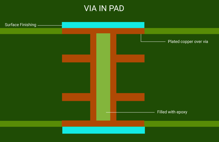
Understanding via in pad in PCB-types, advantages, process, filling ...
PCB Via: An Ultimate Guide
 www.nextpcb.com
PCB Via: An Ultimate Guide
Via-In-Pad Guidelines For PCBs | Electronic Design
 www.electronicdesign.com
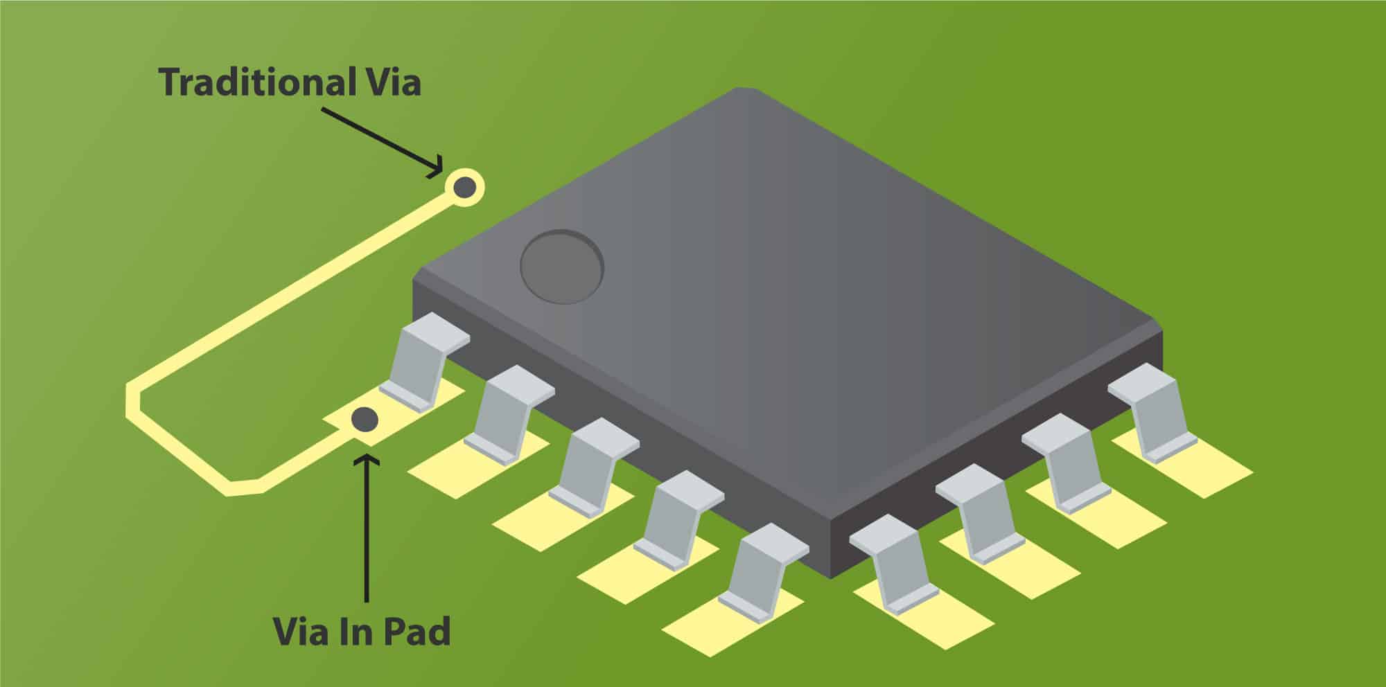
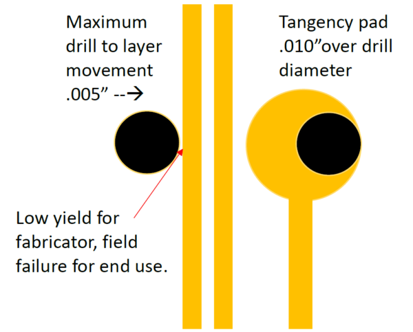
Via-In-Pad Guidelines for PCBs | Electronic Design
How PADS PCB Design Software Impacts PCB Manufacturing
 hillmancurtis.com
How PADS PCB Design Software Impacts PCB Manufacturing
Via In Pad (VIP) In PCB Design - Shady Electronics
 shadyelectronics.com
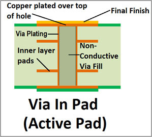
Via in Pad (VIP) in PCB Design - Shady Electronics
Lifted Pads On PCBs - Causes, Repairs, And Prevention - GlobalWellPCBA
 www.globalwellpcba.com
Lifted Pads on PCBs - Causes, Repairs, and Prevention - GlobalWellPCBA
Understanding Via In Pad In PCB-types, Advantages, Process, Filling
 www.pcbaaa.com
Understanding via in pad in PCB-types, advantages, process, filling ...
Removing Non-Functional Pads And Routing Conductors - Summit Interconnect
 summitinterconnect.com
Removing Non-Functional Pads and Routing Conductors - Summit Interconnect
PCB Via Size And Pad Size Guidelines | Zach Peterson | Blog | Altium
 resources.altium.com
PCB Via Size and Pad Size Guidelines | Zach Peterson | Blog | Altium ...
Via-in-Pad For Dense PCB Assemblies - VSE
 www.vse.com
Via-in-Pad for Dense PCB Assemblies - VSE
PCB Pad – A Basic Guide For Beginners - Mainpcba One-stop PCB Assembly
 www.mainpcba.com
PCB pad – a basic guide for beginners - Mainpcba One-stop PCB Assembly ...
How Non-functional Pads Affect Your PCB Design | PCB Routing
 resources.altium.com
How Non-functional Pads Affect Your PCB Design | PCB Routing
Via In Pad (VIP) In PCB Design - TavoTech
 tavotech.com
Via in Pad (VIP) in PCB Design - TavoTech
Lifted Pads On PCBs - Causes, Repairs, And Prevention - GlobalWellPCBA
 www.globalwellpcba.com
Lifted Pads on PCBs - Causes, Repairs, and Prevention - GlobalWellPCBA
Free Via-in-Pad On 6-20 Layer PCBs With POFV
Free Via-in-Pad on 6-20 Layer PCBs with POFV
Via In Pad Guidelines | PCB | Maker Pro
 maker.pro
Via in Pad Guidelines | PCB | Maker Pro
Via In Pad In Pcb Design Manufacturing Sierra Circuit - Vrogue.co
 www.vrogue.co
Via In Pad In Pcb Design Manufacturing Sierra Circuit - vrogue.co
Via-in-pad Guidelines For Printed Circuit Boards (PCBs)
 www.analogictips.com
Via-in-pad guidelines for Printed Circuit Boards (PCBs)
Free Via-in-Pad On 6-20 Layer PCBs With POFV
Free Via-in-Pad on 6-20 Layer PCBs with POFV
Removing Non-Functional Pads And Routing Conductors - Summit Interconnect
 summitinterconnect.com
Removing Non-Functional Pads and Routing Conductors - Summit Interconnect
PCB Vias: Types & Design Best Practices | Reversepcb
 reversepcb.com
PCB Vias: Types & Design Best Practices | Reversepcb
Via In Pad (VIP) In PCB Design - TavoTech
 tavotech.com
Via in Pad (VIP) in PCB Design - TavoTech
Pcb Designs High-speed Design Guidelines For Pcbs Using Vias-in-pad For
 www.alibaba.com
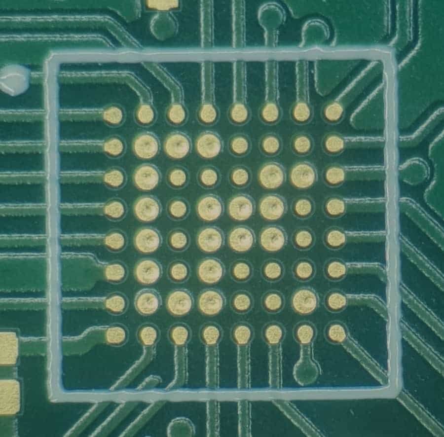
Pcb Designs High-speed Design Guidelines For Pcbs Using Vias-in-pad For ...
Understanding Via In Pad In PCB-types, Advantages, Process, Filling
 www.pcbaaa.com
Understanding via in pad in PCB-types, advantages, process, filling ...
Understanding via in pad in pcb-types, advantages, process, filling .... via in pad (vip) in pcb design. pcb vias: types & design best practices